We are looking forward to hearing from you!
TEL. 03−3262-4296
2-5-10 Kudan-Minami Chiyoda-Ku Tokyo 102-0074 Japan
Products & ServiceSERVICE&PRODUCTS
「CZ silicon wafer」
Diameter: 1 inch - 450 mm
Type: P, N
Orientation: <100>, <111>, <110>, <112>, <510>
*Special orientations are available, depending on the diameter.
Resistivity: subject to your request
Finish: subject to your request
Thickness: subject to your request
Particle size: subject to your request
*We can offer bare wafers, diffused wafers, SOI, EPI, patterned wafers
etc.
*We can arrange various services including cutting, film coating, dicing,
thinning etc.
*We can provide various grade wafers & materials such as prime, lithography,
test, dummy, coinroll, scrap, powder, ingots etc.
*We can offer small quantities for Universities, R&D purposes etc.
![]() The fllowing wafer is available.
The fllowing wafer is available.
![]() 12inch EPI <110> wafer (Rare)
12inch EPI <110> wafer (Rare)
Diameter:12inch
Thickness:775+/-25um
Type:P
Orientation:<110>
Resistivity:0.005-0.01 ohm cm
Finish: Double side Polished
Notch
Package: 25pcs in seald cassete
*One side has EPI film.
*These wafers were made in 2006, but Orientation is rare <110>.
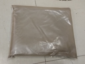
![]() Silicon Powder
Silicon Powder
Purity: 5N UP
Size: 100 mesh Under
Package: 1kg/pack
*Remark:Fe: approx. Max.2ppm Cr: approx.Max.1ppm Mg: approx.Max.0.5ppm Ni:
approx.Max.0.5ppm
バナースペース
ENATEK LTD.
2-5-10 Kudan-Minami Chiyoda-Ku Tokyo 102-0074 Japan
TEL 81-3-3262-4296
FAX 81-3-3262-4048
Osaka Sales Office
3-11-26 Nishinakajima Yodogawa-ku Osaka-shi Osaka 532-0011 JAPAN
TEL 81-6-6307-5495
FAX 81-6-6307-5496